CNT active matrix makes flexible imager
作者:中國(guó)科學(xué)院成都有機(jī)化學(xué)有限公司 來(lái)源:http://www.sikpqwc.cn 日期:2013-11-27 09:02:06
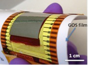
Researchers at the University of California, Berkeley, and the Lawrence Berkeley National Laboratory have succeeded in fabricating mechanically flexible imagers using nanotube-based active-matrix backplanes. The devices, which can image in both the visible and X-ray range, could be used to make large-area flexible sensor networks for a variety of imaging applications, such as interactive surfaces and displays that can be pasted onto a host of surfaces and objects. The devices that work in the X-ray part of the spectrum might find use in portable medical imaging too.
< 上一篇 美國(guó)研制出世界首片碳納米管中央處理器...碳導(dǎo)線助力機(jī)器人產(chǎn)業(yè) 下一篇 >
 川公網(wǎng)安備 51010702000618號(hào)
主站蜘蛛池模板:
欧美大片欧美毛片大片
|
亚洲国产欧美日韩第一香蕉
|
亚洲美女视频在线
|
亚洲欧美中文日韩在线v日本
|
成人男女网18免费0
成人男女网18免费看
|
亚洲韩国欧美一区二区三区
|
国产永久免费高清动作片www
|
精品国产免费第一区二区三区日韩
|
久久中文字幕亚洲精品最新
|
久久视频精品线视频在线网站
|
亚洲国产精品自产拍在线播放
|
九九九精品视频免费
|
国产三级高清
|
久久99视频精品
|
久揄揄鲁一二三四区高清在线
|
欧美自拍在线
|
亚洲欧美日本国产
|
午夜影院0606
|
看一级特黄a大片国产
|
在线国产区
|
亚洲风情第一页
|
欧美一级特黄aa大片在线观看免费
|
国产成人免费手机在线观看视频
|
亚洲一区高清
|
成人在线观看国产
|
久久99精品久久久久久
|
欧美成人看片一区二区三区
|
欧美在线一区二区三区精品
|
在线第一页
|
久久综久久美利坚合众国
|
国产欧美日韩视频在线观看一区二区
|
思思91精品国产综合在线
|
国产黄色三级网站
|
亚洲狠狠ady亚洲精品大秀
|
久久久久久国产精品视频
|
久久羞羞
|
天堂mv亚洲mv在线播放9蜜
|
欧美日韩视频一区二区在线观看
|
国产精品久久久久久久久99热
|
国产成人精品.一二区
|
国产成人免费片在线观看
|
川公網(wǎng)安備 51010702000618號(hào)
主站蜘蛛池模板:
欧美大片欧美毛片大片
|
亚洲国产欧美日韩第一香蕉
|
亚洲美女视频在线
|
亚洲欧美中文日韩在线v日本
|
成人男女网18免费0
成人男女网18免费看
|
亚洲韩国欧美一区二区三区
|
国产永久免费高清动作片www
|
精品国产免费第一区二区三区日韩
|
久久中文字幕亚洲精品最新
|
久久视频精品线视频在线网站
|
亚洲国产精品自产拍在线播放
|
九九九精品视频免费
|
国产三级高清
|
久久99视频精品
|
久揄揄鲁一二三四区高清在线
|
欧美自拍在线
|
亚洲欧美日本国产
|
午夜影院0606
|
看一级特黄a大片国产
|
在线国产区
|
亚洲风情第一页
|
欧美一级特黄aa大片在线观看免费
|
国产成人免费手机在线观看视频
|
亚洲一区高清
|
成人在线观看国产
|
久久99精品久久久久久
|
欧美成人看片一区二区三区
|
欧美在线一区二区三区精品
|
在线第一页
|
久久综久久美利坚合众国
|
国产欧美日韩视频在线观看一区二区
|
思思91精品国产综合在线
|
国产黄色三级网站
|
亚洲狠狠ady亚洲精品大秀
|
久久久久久国产精品视频
|
久久羞羞
|
天堂mv亚洲mv在线播放9蜜
|
欧美日韩视频一区二区在线观看
|
国产精品久久久久久久久99热
|
国产成人精品.一二区
|
国产成人免费片在线观看
|